The Importance of Thorough Wafer Cleaning
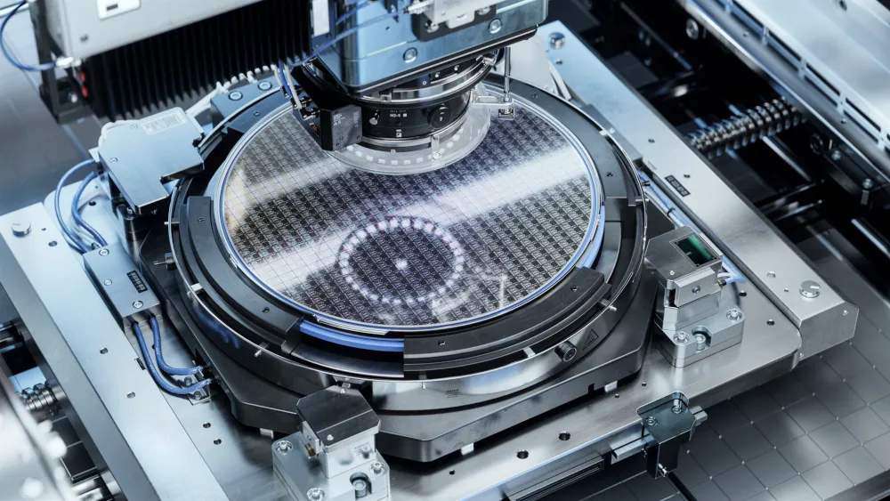
In optical lithography, a light-sensitive photoresist is applied to the substrate. A photomask containing the desired pattern selectively exposes parts of the resist. The exposed areas undergo a chemical change, after which the pattern is transferred onto the wafer through etching, deposition, or ion implantation processes.
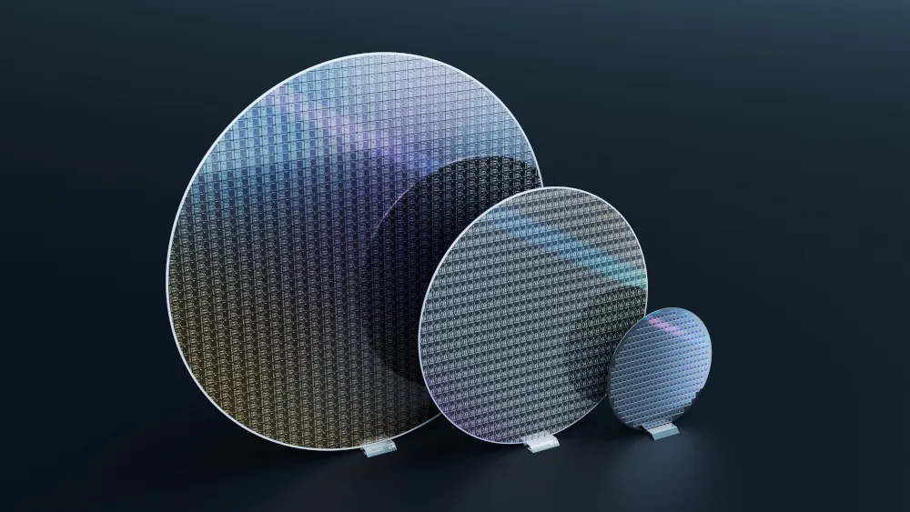
After this process, complete removal of the photoresist is essential. This typically occurs in three stages:
-
Stripping the photoresist
-
Chemical cleaning to remove remaining residues
-
Precise post-processing and passivation of the surface for the next process step
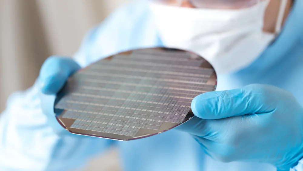
If residues remain, they cause pattern deviations or contamination that affects subsequent processing steps. This can lead to defective circuits, reduced performance, or lower yield.
A reliable detection method is therefore required to identify even unknown or invisible residues during the cleaning process.
Infrared Imaging Reveals Invisible Residues
Infrared cameras are ideal for detecting these contaminants because they visualize differences in thermal emission.
The varying emissivity properties of residues and cleaning agents create thermal contrast that cannot be seen in the optical spectrum. This makes even microscopic residues distinguishable, enabling operators to clean more effectively.
The Optris PI 640 infrared camera is a high-precision thermal imager with a resolution of 640 × 480 pixels, making it possible to detect even minimal thermal deviations.
With the PIX Connect software, users can analyze data in real time and easily integrate the system into existing inspection or cleaning setups.
Its compact size allows effortless integration in confined environments. A range of optics is available — for example, the 60° lens, ideal for monitoring entire reaction chambers or substrate surfaces within a single field of view.
Supporting Lithography and Quality Assurance
By using high-resolution infrared cameras, lithography processes can be better controlled and thoroughly documented.
All relevant data is recorded and forms the basis for quality analysis and process optimization. Deviations or incomplete cleaning are made immediately visible in the infrared image.
The Optris team actively supports customers during implementation. Engineers visit facilities on-site, test configurations, and ensure the cameras are optimally configured. This hands-on guidance enables seamless integration of infrared imaging into semiconductor manufacturing.
Optris’ ongoing technical support ensures a reliable and long-term partnership, with continuous optimization of measurement processes.